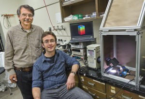
Researchers at the U.S. Department of Energy (DOE)’s Lawrence Berkeley National Laboratory (Berkeley Lab) and the University of California (UC) Berkeley recently announced they have developed a new technology that would enable cheap, high-efficiency solar cells to be made from almost any semiconductor material, including more abundant materials such as metal oxides, sulfides and phosphides. Those materials hitherto have been considered unsuitable for solar cells because it is difficult to tailor their properties by chemical means.
Solar cells convert sunlight into electricity using semiconductor materials that exhibit the photovoltaic effect, that is, they absorb photons and release electrons that can be channeled into an electrical current. Currently photovoltaic technologies rely on scarce and expensive semiconductors, such as large crystals of silicon, or thin films of cadmium telluride or copper indium gallium selenide, that are tricky or expensive to fabricate into devices.
“It’s time we put bad materials to good use,†said physicist Alex Zettl, who led this research along with colleague Feng Wang. “Our technology allows us to sidestep the difficulty in chemically tailoring many earth abundant, non-toxic semiconductors and instead tailor these materials simply by applying an electric field.†Zettl is the corresponding author of a paper describing this work in the journal Nano Letters. The paper is titled Screening-Engineered Field-Effect Solar Cells. Co-authoring it were William Regan, Steven Byrnes, Will Gannett, Onur Ergen, Oscar Vazquez-Mena and Feng Wang.

The new technology is called screening-engineered field-effect photovoltaics (SFPV) because it utilizes the electric field effect, a well understood phenomenon by which the concentration of charge-carriers in a semiconductor is altered by the application of an electric field. With the SFPV technology, a carefully designed partially screening top electrode lets the gate electric field sufficiently penetrate the electrode and more uniformly modulate the semiconductor carrier concentration and type to induce a p-n junction. This enables the creation of high quality p-n junctions in semiconductors that are difficult if not impossible to dope by conventional chemical methods.
Under the SFPV system, the architecture of the top electrode is structured so that at least one of the electrode’s dimensions is confined. In one configuration, working with copper oxide, the Berkeley researchers shaped the electrode contact into narrow fingers; in another configuration, working with silicon, they made the top contact ultra-thin (single layer graphene) across the surface. With sufficiently narrow fingers, the gate field creates a low electrical resistance inversion layer between the fingers and a potential barrier beneath them. A uniformly thin top contact allows gate fields to penetrate and deplete/invert the underlying semiconductor. The results in both configurations are high quality p-n junctions.
“Solar technologies today face a cost-to-efficiency trade-off that has slowed widespread implementation,†added Zettl. “Our technology reduces the cost and complexity of fabricating solar cells and thereby provides what could be an important cost-effective and environmentally friendly alternative that would accelerate the usage of solar energy.â€
The researchers also demonstrated the SFPV effect in a self-gating configuration, in which the gate was powered internally by the electrical activity of the cell itself.
Source: Berkeley Lab


